Node Selection: Micron Skips 10th-Generation NAND
2026-10-23
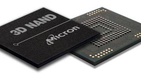
Micron confirmed at its 2026 Technology Webinar that it will skip its originally planned 10th-generation NAND and jump directly from its current 276-layer G9 to G11. G11 stacks more than 400 layers, uses wafer-to-wafer bonding, delivers areal storage density about twice that of G9, raises I/O speed by up to 1.5x, cuts energy per bit of data transfer by more than 25%, and is scheduled to enter capacity ramp in the second half of 2027.
Micron President and Chief Technology and Product Officer Scott DeBoer called it "the world's most advanced NAND" and explained that the generation skip is because this memory has been specifically optimized for future AI products.
Deeper Reasons for the Skip
G9 entered mass production in July 2024, debuting in the 2650 client SSD with 276 layers and a transfer rate of 3.6GB/s. From G7 to G9, Micron led across three consecutive nodes, and under a conventional path it should have advanced to a 300-layer-class G10. Instead, G10 was dropped entirely and replaced by the larger leap to G11.
This choice reflects that, at a stage when AI storage demand is rapidly fragmenting, incremental layer increases may not be the most effective way to invest. Rather than spreading engineering resources across an intermediate node, Micron concentrated bonding process, cell pitch, and energy-efficiency optimization on a node aimed at AI workloads.
Micron also disclosed two AI-class NAND designs: an SLC-based GPU-direct high-IOPS product, and a bandwidth-optimized product similar to the HBF definition, corresponding respectively to low-latency access and high-bandwidth throughput AI scenarios.
400-Layer Threshold and Different Paths
 The 400 layers is becoming a key dividing line in 3D NAND competition. Samsung's V10 takes a wafer-bonding plus low-temperature etch route; SK hynix has lowered its original 400-layer target to 375 layers and shifted to molybdenum instead of tungsten to address resistance increases at higher layer counts; Kioxia and SanDisk's BiCS10 uses a CBA architecture to advance 332-layer QLC.
Traditional single-pass continuous etching is constrained by wafer warpage and interlayer alignment errors and is difficult to push stably beyond 500 layers, making bonding technology a necessary path rather than an optional one for further density gains. Micron's G11 uses wafer-to-wafer bonding, exceeding 400 layers while maintaining a leading cell pitch.
Supply Chain — SEMICONE ICs
The customized design of AI-class NAND means storage controllers, power management, and signal-chain devices must be adapted in sync. As an IC component distributor, SEMICONE provides rapid allocation of scarce parts and one-stop BOM matching services, helping customers shorten sourcing cycles and reduce supply uncertainty. For in-stock IC parts, see SEMICONE IC distributor.
● AD7711ANZ (ADI) — 24-bit Σ-Δ ADC, 2 channels, integrated PGA and digital filter, 24-DIP
● 6V49205BNLGI (Renesas) — clock generator, maximum output frequency 125MHz, 48-VFQFPN
● BQ79718BQPAPRQ1 (TI) — automotive-grade 18-cell series battery monitor, 64-HTQFP
● TLV3601DCKR (TI) — high-speed comparator, push-pull output, SC70-5 package, 2.4V to 5.5V supply
● VND7020AJTR (ST) — dual-channel intelligent high-side driver, 4V to 28V operating voltage, 22mΩ on-resistance, 45A maximum continuous current, PowerLFSOP package
Email: info@semicone.com
Clock Generator: From PLL Fundamentals to Selection and Procurement
Related Article
A guide covers how clock generators work, eight representative ICs compared, sourcing pitfalls and where to buy.
Clock Generator: From PLL Fundamentals to Selection and Procurement
Qualcomm will begin performance-driven global layoffs in November after annual reviews, with no headcount disclosed.
Global Performance-Driven Layoffs at Qualcomm