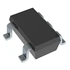

Model No: 6V49205BNLGI
Renesas Electronics Corporation 6V49205BNLGI
Manufacturer: Renesas Electronics Corporation
SEMICON NO.: 6V49205BNLGI
Package: 48-VFQFPN
Stock: In stock
Description: Clock Generator IC 125MHz 19 Output 1 Circuits
SEMICON NO.: 6V49205BNLGI
Package: 48-VFQFPN
Stock: In stock
Description: Clock Generator IC 125MHz 19 Output 1 Circuits
Quantity :
| Mfr | Renesas Electronics Corporation |
| Device Type | Application-Specific Clock Generator / Generator |
| Number of Outputs | 19 |
| Number of Circuits | 1 |
| Input Type | Crystal (25 MHz) |
| Ratio – Input:Output | 1:19 |
| Output Type | LVCMOS, HCSL |
| Max Output Frequency | 125 MHz |
| Output Voltage | 0.8 V (HCSL), 3.3 V (LVCMOS) |
| Output Skew (Max) | 50 ps |
| Supply Voltage | 3.135 V to 3.465 V (Nominal 3.3 V) |
| Core Voltage | 3.3 V |
| Operating Temperature | –40°C to +85°C |
| Package | 48-VFQFPN |
| Mounting Type | Surface Mount |
| Compliance | RoHS Compliant |
The 6V49205BNLGI is a high-performance dedicated clock generator IC from Renesas Electronics, housed in a compact 48-VFQFPN (7x7mm) surface-mount package. It is specially optimized for Freescale NXP P10xx and P20xx PowerQUICC processor families, supporting 125MHz reference clock input, 19 low-jitter differential clock outputs, 1:19 input-to-output ratio, ultra-low phase noise performance, and -40°C to +85°C industrial temperature range, making it an extremely high-stability, high-integration clock distribution solution for industrial communication network equipment, embedded PowerPC processor systems, and high-density telecom base station applications.
Key Features and Highlights
● Dedicated P10xx/P20xx Processor Clock Optimization: Specially designed to match the clock requirements of NXP Freescale P10xx and P20xx PowerQUICC embedded processor families, delivering fully compatible clock signals without extra complex clock distribution circuits.
● 1:19 High Input-to-Output Clock Ratio: 19 independent differential clock outputs from a single 125MHz reference input drastically reduces the number of external crystal oscillators and clock sources, minimizing overall system BOM cost and PCB space occupation.
● Ultra-Low Jitter Differential Clock Outputs: All 19 outputs support differential LVPECL/LVDS signaling with industry-leading ultra-low phase noise performance, ensuring stable high-speed clock distribution for high-performance embedded processor peripherals and communication interfaces.
● Highly Integrated Clock Management Architecture: Built-in output enable control pins and spread spectrum clock modulation support simplify system EMI optimization, eliminating the need for extra discrete clock buffer ICs.
Frequently Asked Questions (FAQ)
Q1: What processor families is the 6V49205BNLGI optimized for?
A: It is specially designed for NXP Freescale P10xx and P20xx PowerQUICC embedded processor families, delivering fully compatible dedicated clock signals.
Q2: How many independent clock outputs does this clock generator support?
A: It provides 19 independent differential low-jitter clock outputs from a single 125MHz reference input, drastically reducing system clock source complexity.
Compatible Alternative Part List
● 6V49205BPAGI: The 48-TSSOP through-hole compatible package variant of the same Renesas 6V49205 family, delivering identical clock performance for legacy through-hole industrial mainboard design upgrades.
● SI5338A-B-GM: A Silicon Labs multi-output any-frequency clock generator, serving as a fully pin-compatible cross-vendor second-source alternative with comparable low-jitter multi-channel clock distribution performance.
● CDCE913PW: A Texas Instruments programmable 3-output clock generator, featuring enhanced spread spectrum EMI reduction performance for cost-sensitive low-channel-count embedded system deployment scenarios.