MediaTek's Strategic Entry into Silicon Photonics: Investment in Ayar Labs
2026-03-02
In February 2026, MediaTek, a leading mobile chip design company, acquired special shares of Ayar Labs, an American silicon photonics enterprise, through its subsidiary Digimoc Holdings Limited. The investment totaled approximately USD 90 million, securing a 2.4% equity stake.
Notably, Ayar Labs boasts an impressive "all-star" roster of shareholders. Semiconductor giants including NVIDIA, the leader in artificial intelligence chips, as well as AMD and Intel, have already invested in the company. In December 2024, Ayar Labs completed a USD 155 million Series D funding round led by Advent Global Opportunities and Light Street Capital, bringing the company's total financing to USD 370 million and pushing its valuation beyond USD 1 billion. MediaTek's entry at this juncture represents not merely a wager on the commercialization of silicon photonics technology, but a strategic maneuver to secure its technological reserves amid the explosive growth of AI computing power.
Silicon Photonics Technology Explained
Silicon Photonics is an innovative technology that integrates optical functions with traditional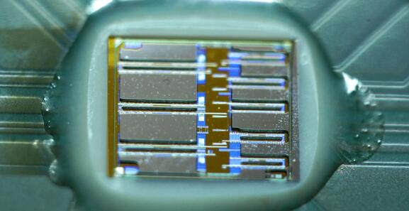 electronic circuits on silicon substrates. It constructs photonic circuits by guiding infrared light along specific pathways through waveguides, enabling high-speed data exchange between chips. Compared with traditional copper wire electrical interconnections, optical signal transmission offers three core advantages: bandwidth density improvements of several orders of magnitude, latency reduced to nanosecond levels, and power consumption decreased by up to 80%.
electronic circuits on silicon substrates. It constructs photonic circuits by guiding infrared light along specific pathways through waveguides, enabling high-speed data exchange between chips. Compared with traditional copper wire electrical interconnections, optical signal transmission offers three core advantages: bandwidth density improvements of several orders of magnitude, latency reduced to nanosecond levels, and power consumption decreased by up to 80%.Ayar Labs' core products include the TeraPHY™ optical I/O chiplet and the SuperNova™ remote light source. TeraPHY stands as the industry's first optical I/O solution based on standard packaging, delivering over 8 Tbps of bidirectional bandwidth per device, with end-to-end latency below 25 nanoseconds and no requirement for forward error correction (FEC). The SuperNova light source adopts the industry-standard ELSFP form factor, providing stable optical signals for optical engines. The combination of these two products enables high-speed optical interconnection between racks and even across racks in AI data centers, connecting thousands of GPUs into unified computing clusters.
Industry Landscape
Ayar Labs established its Hsinchu, Taiwan office in 2025, forging deep collaborations with semiconductor manufacturers such as TSMC and ASE, while also establishing strategic partnerships with ASIC design service providers including Global Unichip Corporation (GUC) and Alchip. This "Silicon Valley innovation plus Taiwan manufacturing" model aims to address the technical challenges of transitioning silicon photonics from laboratory to mass production.
From a competitive perspective, the global silicon photonics market presents a diversified landscape. Traditional giants such as Intel, Cisco, and Inphi dominate the data center transceiver market, while Marvell, Coherent, and Broadcom are accelerating their expansion through mergers and acquisitions. Chinese manufacturers such as Innolight have achieved breakthroughs in the 1.6 Tbps optical module sector, while startups like Lightelligence are exploring commercialization paths in photonic computing chips with integrated memory and processing capabilities.
For MediaTek, the investment in Ayar Labs represents more than a simple financial arrangement—it constitutes a strategic positioning for technology leadership. Against the backdrop of exploding AI computing power demands and the slowing of traditional Moore's Law, silicon photonics technology has emerged as a critical pathway to break through the "power wall" and "bandwidth wall." As giants including NVIDIA, AMD, and Intel continue to increase their investments, and with Co-Packaged Optics (CPO) technology accelerating its deployment in AI data centers, silicon photonics is transforming from an "optional" technology into a "mandatory" one. MediaTek's entry into this space aims to ensure its continued technological leadership in the 6G and edge AI era, avoiding obsolescence in next-gen interconnect architectures.
Semicone Intergrated Components Distributor
Semicone, as a semiconductor component distributor, focuses on providing a complete supply chain solution for the electronics manufacturing industry. In response to the common chip shortage problem faced by customers, Semicone adopts diversified methods such as global sourcing, spot allocation, and alternative solution recommendations to help customers solve the emergency shortage problem. At the same time, Semicone also provides BOM list services, covering component selection, cost optimization, and delivery tracking, to provide comprehensive support for customer needs, significantly shortening the customer's procurement cycle and reducing supply chain risks.
Here are several popular selected ic models:
● XC2S50-4PQ208C: Xilinx Spartan-II series FPGA, using 0.18 micron CMOS process, integrating 50,000 system gates and 140 I/O pins, suitable for medium-density logic design and embedded signal processing applications.
● SN54LS244J: TI classic eight-channel buffer/driver, with tri-state output function, widely used in bus driving and signal isolation scenarios, is the preferred logic device for industrial-grade high-reliability systems.
● ADXL382-1BCCZ-RL7: ADI ultra-low noise 3-axis MEMS accelerometer, with noise density as low as 44 μg/√Hz, supporting 8kHz bandwidth and 520μA low power consumption mode, optimized for industrial status monitoring and edge AI applications.
● LSM6DSRTR: ST high-performance six-axis IMU, integrating 3D accelerometer and 3D gyroscope, supporting AI algorithm embedding and low power consumption mode, designed for wearable devices and industrial IoT motion detection.
Email: info@semicone.com
Price Hike Wave Spreads Across the Board: From Memory to All Chips
SK Hynix and SanDisk Launch HBF Standardization Alliance
Related Article

Ericsson will merge Northeast Asia with Southeast Asia, Oceania and India into one APAC unit and dissolve its enterprise wireless division, effective Jan 1, 2027.
Ericsson Merges Asia-Pacific Regions, Dissolves Enterprise Wireless Division
NVIDIA prepays KYEC to secure US testing capacity. KYEC and its AeternZ subsidiary will build the capacity, repayment offsets future service fees.
NVIDIA Prepayment Lock KYEC's US Testing Capacity