
onsemi EPP Platform: Reconstructing Power Packaging Architecture with 12-Inch Silicon Wafers
2026-09-17
As rack power density in AI data centers continues to climb and efficiency requirements for electric vehicle traction inverters become increasingly stringent, traditional power electronics packaging is approaching its physical limits. On September 16, onsemi officially launched its Embedded Power Platform (EPP), transforming packaging from a passive physical enclosure into an active performance enhancer and using the 12-inch silicon wafer itself as the packaging carrier.
Heterogeneous silicon, silicon carbide (SiC), and gallium nitride (GaN) dies are embedded directly into cavities in the wafer and interconnected through precisely patterned wafer-level copper redistribution layers (RDL) and vertical vias, completely eliminating traditional wire bonding. Because key assembly steps are completed inside a controlled semiconductor fab, cleanroom manufacturing precision can be applied directly to power system integration.
Coordinated Breakthroughs in Electrical and Thermal Performance
Architectural Advantages
The architectural advantages of EPP have already translated into quantifiable benefits in practical applications. In an early solid-state circuit breaker design for AI systems, an EPP-based solution reduced size by about 50% and operating temperature by about 20% compared with conventional designs. For EV traction inverters, EPP can deliver up to 4x higher power density and 15% lower power loss, while its scalable architecture supports a single inverter platform from low-end to high-end, helping automakers reuse designs across vehicle models and reduce R&D and manufacturing costs.
Notably, Subaru has become one of EPP's first early partners and is working with onsemi to evaluate how the platform can support future electrified vehicle architectures. EPP is planned to begin delivering engineering samples to strategic partners in the automotive and AI ecosystems in 2026.
SEMICONE — IC Chip Distribution Services
SEMICONE, as a professional IC chip distributor, serves customers in industrial control, automotive electronics, and communications equipment, providing genuine IC in-stock supply and one-stop BOM supporting services. SEMICONE's core advantages lie in fast delivery enabled by dual warehouse inventory in Shenzhen and Hong Kong, and a professional technical team providing part selection, alternative recommendations, and technical support. Today's hot-selling featured components are as follows:
● PIC16F1827T-I/SS (Microchip) — 8-bit PIC MCU, 32MHz main frequency, 7KB Flash, 384B RAM, 16 I/Os, integrated I2C/SPI/UART and mTouch capacitive touch sensing, SSOP-20 package, suitable for smart home control and industrial sensor nodes.
● MP1479GTF-Z (MPS) — 1A synchronous step-down converter, 4.2V–18V wide input, 800kHz switching frequency, built-in 140mΩ/60mΩ low on-resistance MOSFETs, SOT-563 package, suitable for industrial power supplies and portable devices.
● RC19016AGN1#KB0 (Renesas) — PCIe Gen5/Gen6 fanout buffer, 16 outputs, additive phase jitter only 30fs RMS at 156.25MHz, 64-VFQFPN package, suitable for high-speed clock distribution in data centers.
● ADT7461AARMZ-R (onsemi) — digital temperature sensor, local/remote dual-channel monitoring, accuracy ±1°C, SMBus/I2C interface, 8-MSOP package, suitable for server thermal management and industrial system temperature monitoring.
Email: info@semicone.com
ASML EUV Lithography Expansion: 2028 Capacity Target of 110 Units
Related Article
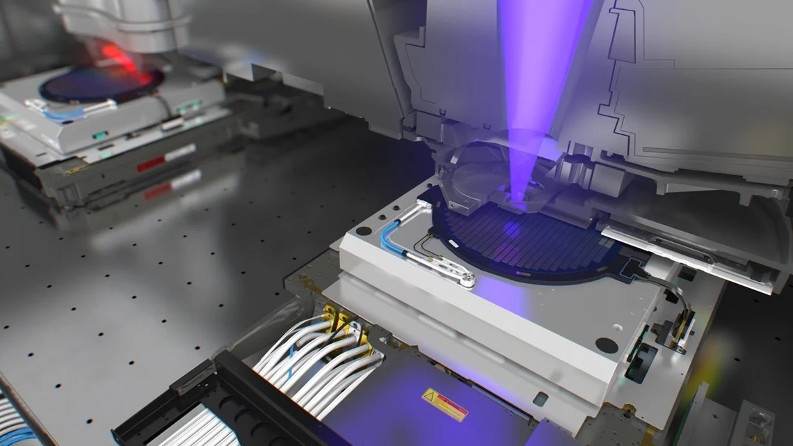
ASML eyes 110 EUV units by 2028; 2027 sold out. AI drives TSMC, Samsung, Intel demand. Tech upgrades boost output.
ASML EUV Lithography Expansion: 2028 Capacity Target of 110 Units
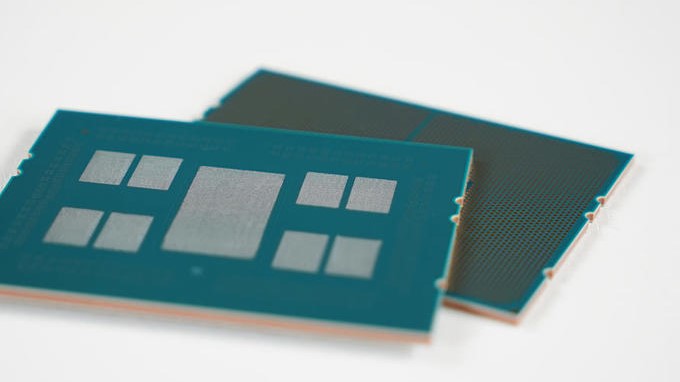
Samsung & Qualcomm develop organic-bridge 2.1D packaging, replacing silicon bridges to cut costs and avoid Intel EMIB patents.
Samsung Electro-Mechanics and Qualcomm Develop Organic-Bridge 2.1D Packaging

