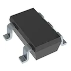
Model No: RC19016A100GN1
Renesas Electronics Corporation RC19016A100GN1
Manufacturer: Renesas Electronics Corporation
SEMICON NO.: RC19016A100GN1
Package: 64-VFQFPN
Stock: In stock
Description: SBuffer PCIe 1:16 100 Ω 400 MHz
SEMICON NO.: RC19016A100GN1
Package: 64-VFQFPN
Stock: In stock
Description: SBuffer PCIe 1:16 100 Ω 400 MHz
Quantity :
| Mfr | Renesas Electronics Corporation |
| Device Type | PCI Express (PCIe) Gen5/Gen6 Fanout Buffer |
| Product Family | RC190xx / RC190 Series |
| Input : Output Ratio | 1:16 |
| Output Impedance | 100 Ω |
| Max Frequency | 400 MHz |
| Max In-Out Propagation Delay | < 1.5 ns |
| Input Type | HCSL, LVDS |
| Output Type | LP-HCSL |
| Supply Voltage | 2.97 V to 3.63 V |
| Operating Temperature | -40°C to +105°C |
| Package | 64-VFQFPN |
| Mounting Type | Surface Mount |
| Compliance | RoHS Compliant |
The RC19016A100GN1 is a high-performance 16-output QBUFFER clock buffer IC from Renesas Electronics, housed in a compact surface-mount package. It features 100Ω on-chip output termination, supports 3.0V to 3.6V single-supply operation, delivers 1.8ns maximum propagation delay and 400MHz maximum input frequency, with full -40°C to +105°C extended industrial temperature range, making it a robust, high-skew-low clock distribution solution for high-speed telecom, server, and industrial high-density digital systems.
Key Features and Highlights
● 16 High-Differential Clock Outputs: 16 independent buffered clock outputs support simultaneous clock distribution to multiple high-speed FPGAs, CPUs, and high-resolution ADCs, eliminating complex fan-out routing on high-density PCBs.
● 100Ω Integrated On-Chip Output Termination: Built-in 100Ω output impedance matching resistors remove the need for external termination components, drastically reducing BOM cost and simplifying high-speed clock signal integrity design.
● Ultra-Low 1.8ns Maximum Propagation Delay: Extremely short maximum propagation delay minimizes clock path skew across all 16 outputs, ensuring tight timing synchronization for high-speed parallel digital systems.
● 400MHz Wide Maximum Input Frequency: Supports up to 400MHz high-speed clock input, fully covering the clock distribution requirements of most high-performance industrial, telecom, and server digital systems.
● 3.0V to 3.6V Wide Supply Compatibility: Natively works with standard 3.3V digital system power rails, perfectly matching the power supply architecture of modern FPGA, MCU, and server motherboard designs.
● 16 High-Differential Clock Outputs: 16 independent buffered clock outputs support simultaneous clock distribution to multiple high-speed FPGAs, CPUs, and high-resolution ADCs, eliminating complex fan-out routing on high-density PCBs.
● 100Ω Integrated On-Chip Output Termination: Built-in 100Ω output impedance matching resistors remove the need for external termination components, drastically reducing BOM cost and simplifying high-speed clock signal integrity design.
● Ultra-Low 1.8ns Maximum Propagation Delay: Extremely short maximum propagation delay minimizes clock path skew across all 16 outputs, ensuring tight timing synchronization for high-speed parallel digital systems.
● 400MHz Wide Maximum Input Frequency: Supports up to 400MHz high-speed clock input, fully covering the clock distribution requirements of most high-performance industrial, telecom, and server digital systems.
● 3.0V to 3.6V Wide Supply Compatibility: Natively works with standard 3.3V digital system power rails, perfectly matching the power supply architecture of modern FPGA, MCU, and server motherboard designs.
Frequently Asked Questions (FAQ)
Q: What is the maximum operating temperature range of this clock buffer?
A: It is fully specified for -40°C to +105°C extended industrial temperature range, supporting stable operation in harsh high-temperature industrial and outdoor telecom deployment environments.
Q: What is the maximum operating temperature range of this clock buffer?
A: It is fully specified for -40°C to +105°C extended industrial temperature range, supporting stable operation in harsh high-temperature industrial and outdoor telecom deployment environments.
Compatible Alternative clock buffer List
● RC19016AGN1: The 85Ω on-chip output termination variant of the same 16-output clock buffer, optimized for 85Ω impedance controlled PCB clock routing scenarios.
● CDCLVP1116RHAR: A Texas Instruments 16-output high-performance clock buffer, serving as a fully pin-compatible cross-vendor second-source alternative with equivalent 400MHz maximum input frequency.
● RC19008A100GN1: The 8-output 100Ω termination variant of the same QBUFFER series, offering half the output count for medium-density clock distribution system cost optimization.
● SI53316-B-GM: A Silicon Labs high-performance 16-output clock buffer, featuring integrated jitter attenuation for ultra-low phase noise high-precision clock distribution applications.
● RC19016AGN1: The 85Ω on-chip output termination variant of the same 16-output clock buffer, optimized for 85Ω impedance controlled PCB clock routing scenarios.
● CDCLVP1116RHAR: A Texas Instruments 16-output high-performance clock buffer, serving as a fully pin-compatible cross-vendor second-source alternative with equivalent 400MHz maximum input frequency.
● RC19008A100GN1: The 8-output 100Ω termination variant of the same QBUFFER series, offering half the output count for medium-density clock distribution system cost optimization.
● SI53316-B-GM: A Silicon Labs high-performance 16-output clock buffer, featuring integrated jitter attenuation for ultra-low phase noise high-precision clock distribution applications.