TI TPSM Series Power Module Selection Guide
2026-08-17
Texas Instruments' (TI) TPSM family of synchronous buck power modules, with their highly integrated architecture, has become a preferred choice in industrial automation, communications infrastructure, automotive electronics, and AI acceleration. The series covers a wide input voltage range from 2.4 V to 65 V and output currents from 600 mA to 30 A, providing systematic solutions for various power levels.
Integrated Architecture of the TPSM Series
In traditional DC‑DC designs, engineers must independently select inductors, MOSFETs, compensation networks, and repeatedly verify loop stability. TPSM modules, however, pre‑integrate the controller, power MOSFETs, inductor, and key passive components into a single package, requiring only external input/output capacitors to complete the power design. This approach brings significant benefits in multiple dimensions:
- It eliminates magnetic component selection and loop compensation, greatly improving design efficiency;
- The internally matched and optimised devices deliver higher efficiency and better EMI performance;
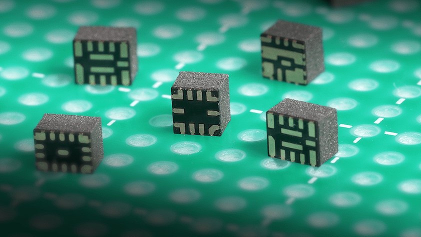
- TI's ongoing packaging innovations – MicroSiP™ for extreme miniaturisation, HotRod™ QFN balancing thermal performance with low EMI, and MagPack™ with bond‑wireless packaging and shielded inductor technology to further shrink solution size and suppress interference – provide differentiated implementation paths for different applications.
Selection by Voltage Class and Application Scenario
1. Low‑Voltage High‑Density Series (Vin ≤ 6 V)
Targeting battery‑powered and space‑constrained applications:
- TPSM8282x family offers 1‑A, 2‑A, and 3‑A options in a MicroSiP™ package, with input voltage from 2.4 V to 5.5 V and quiescent current as low as 4 µA. The standard version supports automatic power‑save mode (PFM) to maintain high efficiency under light loads and extend battery life.
- TPSM8282xA variants adopt forced PWM mode, maintaining continuous conduction under all load conditions to minimise output ripple.
- TPSM8281x family increases current capability to 4 A/6 A, uses MagPack™ packaging, and supports adjustable switching frequencies from 1.8 MHz to 4 MHz.
- TPSM82830x series features DCS‑Control™ topology with an integrated on‑chip noise‑filtering capacitor.
2. Medium‑Voltage General‑Purpose Series (Vin 17 V – 36 V)
- TPSM8291x family (3‑V to 17‑V input, 2‑A/3‑A/4.5‑A/6‑A options) is optimised for noise‑sensitive applications. It incorporates ferrite‑bead filter compensation, achieving output characteristics close to a low‑noise LDO by filtering the internal reference, thus eliminating the need for external LDOs or passive post‑filters.
- TPSM8683x series supports 4.5‑V to 28‑V input and 8‑A output, with D‑CAP3™ control for fast transient response.
- TPSM336x5 series covers 3‑V to 36‑V input, available in 1.5‑A (TPSM33615) and 2.5‑A (TPSM33625) versions.
3. High‑Voltage Wide‑Input Series (Vin ≥ 60 V)
- TPSM656x0 family supports a wide input range of 3.5 V to 65 V and provides 1‑A, 2‑A, and 3‑A output options. It incorporates MINT 2 technology with integrated spread‑spectrum (DRSS) and slew‑rate control to reduce peak emissions.
- TPSM365R6 series operates from 3 V to 65 V input, delivers 600 mA output, and withstands 70‑V transients.
Key Selection Considerations
When choosing from the rich TPSM portfolio, designers should focus on input voltage compatibility, output current margin, EMI/noise sensitivity, and package/thermal requirements.
Input voltage is the primary filter – ensure the module matches the target power bus (e.g., 5‑V, 12‑V, 24‑V, or 48‑V systems). Output current should reserve adequate headroom for peak loads. For EMI and noise, applications such as medical equipment, test & measurement, and telecom infrastructure should prioritise low‑noise series like the TPSM8291x. In terms of package and thermal performance, HotRod™ QFN suits high‑thermal‑demand scenarios, while MagPack™ is ideal for extreme miniaturisation.
In summary, TI's TPSM series power modules, with their highly integrated architecture that encapsulates controller, MOSFETs, inductor, and passives in one package, drastically simplify the DC‑DC design flow. By shifting the design focus from component‑level tuning to system‑level innovation, the TPSM family offers efficient, reliable, and easy‑to‑use power solutions for industrial, automotive, communications, and AI‑accelerator applications.
Email: info@semicone.com
DJI vs. U.S. Department of Defense: Case Remanded for Retrial
From MCUs to Analog Chips, NSING and ADI Raise Prices Again
Related Article

A guide covers how clock generators work, eight representative ICs compared, sourcing pitfalls and where to buy.
Clock Generator: From PLL Fundamentals to Selection and Procurement

Qualcomm will begin performance-driven global layoffs in November after annual reviews, with no headcount disclosed.
Global Performance-Driven Layoffs at Qualcomm