TSMC's Advanced Process Layout in Japan: A $13.9 Billion Investment in 6nm Chip Production
2025-10-27
TSMC, a global leader in semiconductor manufacturing, has been significantly increasing its overseas investment efforts in recent years, particularly in the United States and Japan. This strategic layout not only reflects TSMC's global vision but also has a profound impact on the distribution of the global semiconductor industry. This article will delve into TSMC's investment plans in Japan, especially the construction of its second wafer factory in Kumamoto Prefecture, and the significance of this move for Japan's semiconductor industry.
TSMC's Overseas Strategic Layout
In Japan, TSMC's investment has also attracted significant attention. In 2022, TSMC constructed its first wafer factory in Kumamoto Prefecture, primarily producing chips with processes ranging from 28nm to 12nm. The construction of this factory marked TSMC's initial layout in Japan, laying the foundation for further investment.
Construction of the Second Wafer Factory in Kumamoto Prefecture
In October 2025, TSMC officially confirmed that it had reached an agreement for its second wafer factory in Kumamoto Prefecture, which is expected to begin operations in 2027. This factory, located to the east of the first factory in Kumamoto, covers an area of 69,000 square feet and is projected to create over 1,700 job positions, with both factories combined employing approximately 3,400 employees.
The chip process of this wafer factory has been significantly upgraded, reaching the 6nm node directly. This level of process is considered advanced globally and is mainly used in high-end industries such as autonomous driving and artificial intelligence (AI). Previously, the most advanced process that could be produced locally in Japan was at the 28nm node; TSMC's move has elevated Japan's local chip process by two to three generations.
Due to the significant upgrade in process, the investment scale for this project is also quite substantial. The investment for the second wafer factory amounts to $13.9 billion. Adding the $8.6 billion investment for the first factory, the total investment for both factories will reach $22.5 billion. This investment scale will bring a total investment of 3.4 trillion yen to Japan, which is of great significance to Japan's economic development.
To support TSMC's investment project, the Japanese government has also provided substantial subsidies. The Ministry of Economy, Trade and Industry (METI) has allocated 1.2 trillion yen to subsidize the factory's construction. This subsidy, which accounts for nearly half of the total investment, demonstrates the Japanese government's emphasis on and support for the semiconductor industry.
Impact on Japan's Semiconductor Industry
TSMC's investment in Japan not only brings advanced chip manufacturing processes but also presents new opportunities for Japan's local semiconductor industry. Through cooperation with TSMC, Japanese companies can learn advanced manufacturing technologies and management experience, thereby enhancing their competitiveness. Moreover, the operation of TSMC's factories will also drive the development of related industrial chains, promoting an overall upgrade of Japan's semiconductor industry.
From a global perspective, TSMC's investment in Japan also holds significant strategic importance. With the growing global demand for semiconductors, especially in emerging fields such as autonomous driving and artificial intelligence, TSMC's advanced processes will provide strong support for the development of these areas. Additionally, this investment will help alleviate the global semiconductor supply shortage, enhancing the stability and security of the global semiconductor industry.
Conclusion
The construction of TSMC's second wafer factory in Kumamoto Prefecture marks a new phase in its advanced process layout in Japan. This investment not only brings advanced chip manufacturing processes to Japan but also provides new impetus for the upgrade and development of Japan's semiconductor industry. Meanwhile, this strategic layout also reflects TSMC's global vision and sense of responsibility towards the global semiconductor industry. In the future, as the factory is built and begins operations, TSMC's investment in Japan will have a profound impact on the global semiconductor industry landscape.
Semicon Integrated Circuit Chips Supplier
Semicon is a global semiconductor chip distributor, dedicated to providing high-performance and highly reliable IC solutions. Semicon's products are widely used in multiple fields such as industrial control, communication, automotive electronics and consumer electronics. Semicon offers a wide range of ic chips, including memory chips, single-chip microcomputers, power management chips, etc. The following are the popular IC chips selected by Semicon.
● ADP5071ACPZ: A high-performance power management chip, suitable for a variety of electronic devices, providing stable power solutions.
● STM32L412CBU6: A low-power microcontroller featuring high-performance processing capabilities and a wealth of peripheral interfaces, it is widely used in embedded systems.
● EP4CE22F17I7N: An FPGA chip, suitable for complex logic control and high-speed signal processing, and widely used in communication and industrial control fields.
● DRV8353HMRTAT: A high-performance motor driver chip, suitable for a variety of motor control applications, providing efficient and reliable drive solutions.
Email: info@semicone.com
Qualcomm Launches Cloud AI Chips, Entering the Data Center Market
Google and Anthropic Announce a 1-Million-TPU Supply Agreement
Related Article
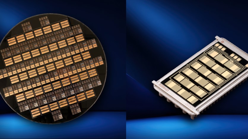
onsemi EPP uses 12-inch silicon wafers to package SiC/GaN power chips, eliminating wire bonding. It cuts AI breaker size 50% and EV loss 15%.
onsemi EPP Platform: Reconstructing Power Packaging Architecture with 12-Inch Silicon Wafers
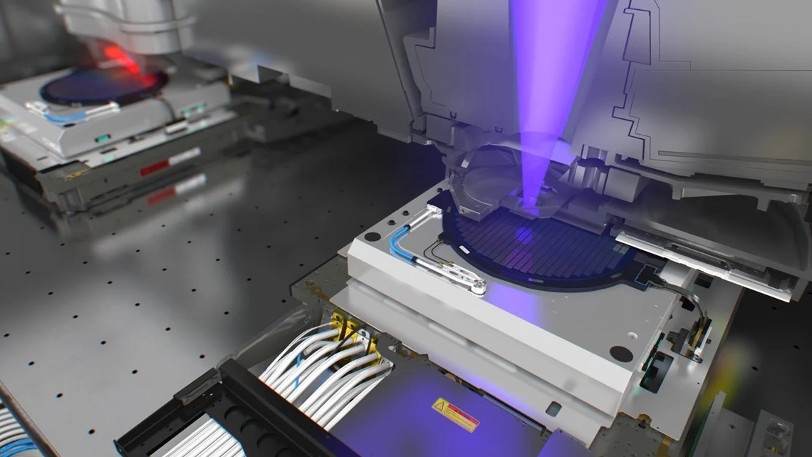
ASML eyes 110 EUV units by 2028; 2027 sold out. AI drives TSMC, Samsung, Intel demand. Tech upgrades boost output.
ASML EUV Lithography Expansion: 2028 Capacity Target of 110 Units